[From the last episode: We looked at the many steps required to dig a swimming pool using only MEMS-like techniques.]
Before we take a look at some specific kinds of sensorsA device that can measure something about its environment. Examples are movement, light, color, moisture, pressure, and many more., let’s talk a bitThe smallest unit of information. It is a shortened form of "binary digit." Since it's binary, it can have only two values -- typically 0 and 1. more about MEMS processing, since it’s incredibly versatile. There are a couple things that are important to how this works: different types of processing and materials properties that might matter.
Bulk and Surface Micromachining
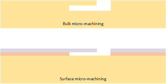
We saw that MEMS, like integrated circuits, are made by depositing and etching materials, with the help of photolithography. But there are different ways to approach this. The two primary ways are referred to as bulk micromachining and surface micromachining. In order to understand the distinction, we need to talk about the notion of a substrate.
We talked about depositing things on a siliconAn element (number 14 in the periodic table) that can be a semiconductor, making it the material of preference for circuits and micro-mechanical devices. wafer. The starting wafer is an example of a substrate: it’s the surface upon which you build things. While silicon is common, you could use, for instance, glass or plastic, depending on what you’re trying to do. Given an analogy to normal construction (buildings etc.), you can think of a substrate as the ground.
With surface micromachining, you deposit materials first on the substrate and then etch them to build structures. In this case, the substrate’s role is simply to hold everything up. Building an above-ground pool is analogous to this. Note that if silicon is a part of what you add above the substrate, it’s usually polycrystalline silicon – that is, it’s not all one big crystal, but a mish-mash of small crystals.
With bulk micromachining, you’re building structures into the substrate – like digging an in-ground pool (which is what we did last time). Now the substrate matters, since it does more than hold up the structures – it forms part of the structures. If the substrate is silicon, then it’s the wafer itself – and it’s a single crystal.

So why would you do one instead of the other? Well, you can make smaller structures using surface micromachining because you’re laying down thin films of materials. On the other hand, because a silicon wafer is one big crystal, it’s strong and allows you to build more precisely.
Different Ways of Etching
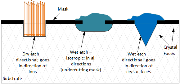
We talked about the different ways of etchingA means by which materials can be removed from a silicon wafer., including wet and dry (plasmaA fourth state of matter (the other three being solid, liquid, and gas). It’s characterized by atoms being stripped of their electrons; it takes a lot of energy to get into this state.) etch. These etching types can be directional (anisotropic) or non-directional (isotropic). Directional means that the etch goes primarily in one direction. Dry etch is directional because the ions bombard the wafer in a specific direction; it’s like they’re drilling in that direction.
Wet etch can be isotropic or directional. If isotropic, it goes in all directions, typically undercutting the masked area. But when they’re directional, it’s different from what happens with dry etch. Here you don’t have ions pounding in one direction; you simply have a liquid etchant lying on the silicon. It turns out that silicon etches at different rates in different directions. Because it’s a crystal, it has crystal faces – like a diamond. Some faces etch faster than others based on how strongly the silicon atoms are attached in those directions.
When you buy a wafer, you order one having a specific crystal orientationThe direction someone or something is facing. This may be different from the direction of motion.. That sets which directions those faces point in. In many cases, the preferred etching direction is down at an angle. By etching, you end up with a so-called V-groove. The following drawing illustrates these different etching methods. (But, unlike the drawing, you can’t do all three types at once with the same maskA piece of glass with a pattern on it that is used to block light or let light pass through in different places. Used for photolithography. set; you’d have to do them separately. I cheated in the drawing.)

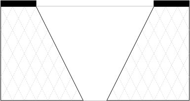
As an example, if you do a V-groove all the way through the substrate, you can create a precise, tiny hole on the backside of the substrate. This is how folks make ink-jet printer nozzles. (It looks from the drawing like we’ve separated the substrate into two pieces, but picture it as sort of a funnel – it’s a hole, so the substrate is connected in front of and behind what we’re looking at.)

Microfluidics
Another variant is an area called microfluidics. As the name suggests, you can think of this as a miniaturized set of pipes. Many devices intended for healthcare use this approach. For instance, you can run blood through it and analyze it for all kinds of problems – or, at least, that’s the promise. It’s still in the early stages.
As one example, a research institute in Belgium called Imec has developed a cell sorter that can take blood and isolate specific cells. It’s pretty complicated stuff once it’s all put together, but you can find more info here.
Material properties
Finally, you have to choose both substrate and added materials carefully. Substrate matters for bulk micromachining, and it also affects cost. With surface micromachining or with other layers added to bulk-micromachined wafersIn the context of making circuits, sensors, and actuators, a thin, round slice of pure silicon. Multiple devices will be made on it; it will then be sliced up to separate the individual chips., you also have to pay attention to important material properties.
- How it etches: if you want one layer to stick around while another one is etched away, then you need to make sure that you use a material that won’t etch away with the other one.
- PiezoelectricityA natural phenomenon with certain materials where, if you stress them mechanically (bend, for example), they exhibit an electrical change. The reverse also occurs: if you apply an electric field, they will bend or deform in some way. The effect is tiny, but measurable.: we mentioned this one before. These materials turn mechanical motion into electrical signals, and vice versa.
- Thermal characteristics: what happens when the layer heats up? Does it want to bend up, for example? Then perhaps you might want to add another layer that bends down to counteract the bending. (That’s way over-simplified, but you get the picture.)
With this completing our general discussion of MEMS, we can now start looking at some specific kinds of sensors – along with some important sensor notions.

Leave a Reply