[From the last episode: we looked at different ways of removing material from a wafer.]
So far we’ve seen that we can add materials to a wafer and we can remove them. But, if those are our only tools, then it’s not particularly useful, since we’re covering a whole wafer with some material and then removing it from the whole wafer. What’s the point?
That’s why we need one more process: a way to be more selective about adding here or removing there so that we can build structures. It’s called photolithographyA way of creating patterns on a silicon wafer for selective deposition or etching. You can think of it as taking a picture of the pattern and having it show up on the wafer. In the industry, photolithography is often abbreviated as lithography., often shortened to lithography, or even just litho. Basically, it means using the wafer as photographic film (for those of you who lived before the age of digital cameras) and creating a picture on it. But with real photographs, you have color and shading and lots of nuance. For wafersIn the context of making circuits, sensors, and actuators, a thin, round slice of pure silicon. Multiple devices will be made on it; it will then be sliced up to separate the individual chips., it’s not so subtle: either something sees light or it doesn’t. There’s no in-between. Let’s see how this works.
Hard to Resist
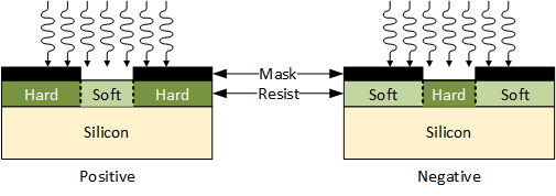
The critical ingredient in this process is material that reacts to light; it’s called photoresist, or just resist. It’s like the active layer on photographic film. It changes its nature when exposed to light. So if you have a way of blocking the light some places but not others, then you create a pattern. That way of blocking light is called a photomaskA piece of glass with a pattern on it that is used to block light or let light pass through in different places. Used for photolithography., or, more commonly, simply a mask.
![]()
By Peellden – Own work, CC BY-SA 3.0, https://commons.wikimedia.org/w/index.php?curid=15946829
The mask in the photo above is for an older, smaller wafer with 20 different chipsAn electronic device made on a piece of silicon. These days, it could also involve a mechanical chip, but, to the outside world, everything looks electronic. The chip is usually in some kind of package; that package might contain multiple chips. "Integrated circuit," and "IC" mean the same thing, but refer only to electronic chips, not mechanical chips. on it. (Each chip on the wafer is called a die, and, although the industry steadfastly refuses to acknowledge this, the plural is dice, not “die” or “dies.”) It consists of black regions and transparent regions. The black regions block the light; the transparent regions let the light through.
What happens when the light hits the resist depends on the kind of resist and material used to deliver it. With negative resists, the developer won’t remove the resist unless it’s been exposed to light. The exposed parts get “softer” and are removed by the resist. With positive resist, the resist is already “soft” and the light hardens it, so the developer removes resist that has not been exposed to light.

Selective Adding and Removing
So now we can create patterns by masking them out. Let’s say we want to create a hole in the siliconAn element (number 14 in the periodic table) that can be a semiconductor, making it the material of preference for circuits and micro-mechanical devices. that goes into (but not all the way through) the wafer. We do that using the following steps (using positive resist), and illustrated in the animation that follows:
- Start with a silicon wafer
- Deposit resist onto the wafer
- Put the mask over the wafer
- Expose the wafer to light
- Remove the mask
- Develop the resist
- Etch the silicon. This assumes that the etch won’t affect the resist. (There are ways of dealing with that if it will; we won’t worry about that.)
- Remove the resist
Notice that the final shape depends on how we do the etchingA means by which materials can be removed from a silicon wafer.. If we want nice vertical walls in the hole, then we need to etch in a way that just goes straight down in; plasmaA fourth state of matter (the other three being solid, liquid, and gas). It’s characterized by atoms being stripped of their electrons; it takes a lot of energy to get into this state. etch is better at this. If we use wet etch, then it etches in all directions, including under the resist, hollowing out more than we want (but there are times when that is exactly what we want).
You can see that all we did was deposit materials, remove materials, and used photolithography to define where we wanted what. The pattern on the mask above is more typical of what’s going onto the wafer, although bear in mind that that’s a really, really old photo – there’s so much more in so little space these days. In addition, that photo represents pieces of a circuit, not something mechanical.
So we now have the basic tools – depositionA means by which materials can be added to a silicon wafer., etching, and litho – that we need to make mechanical structures in silicon. We’ll explore that further in the next weeks.

Leave a Reply